
Cactus Semiconductor is an ISO 9001:2008 certified supplier of low-power mixed-signal Application Specific Integrated Circuits (ASICs), specializing in miniaturized portable and implantable medical devices. The company leverages its systems expertise and vast experience with ultra-low-power integrated circuit design to provide optimal solutions for medical device ASICs. Expertise is also leveraged for a variety of portable and wearable device applications for which size, weight, and power are critical factors. Below is our interview with Andy Kelly, IC/System Architect at Cactus Semiconductor Inc.:

Q: What exactly does Cactus Semiconductor do?
A: Cactus Semiconductor primarily develops full-custom ASICs. This differs from the majority of semiconductor companies who develop and sell standard-product ICs. As the name suggests, Application Specific Integrated Circuits (ASICs) are developed for a single, specific application, while the goal for most standard-product integrated circuits (ICs) is to compromise features and performance to maximize the number of potential applications for each IC.
The design process for ASICs is very similar to that for standard-product ICs. The process starts with the development of a set of requirements for the IC design, followed by a detailed “Design-To” specification. Once that is agreed to, the design team uses a variety of industry-standard Electronic Design Automation (EDA) tools, along with vast knowledge and experience to create analog, digital, and mixed-signal integrated circuits that meet the specified requirements. Design files are then sent to a silicon wafer foundry, where lithography masks are produced and used in the fabrication of the silicon wafers that contain the custom ICs. Prototype samples are then assembled into one of a wide variety of optional IC packages, and electrically tested to validate all the required features and performance. Once the validation is complete, the ICs are mass-produced and sold to the customer to be used as critical components in their final products.
Since our founding in 2002, we have developed ASICs for more than a dozen medical device applications, as well as several commercial & industrial applications, such as energy harvesting and wireless communications. We have also developed an Application Specific Standard Product (ASSP) to help customers jump-start the development of new Neuro-Stimulation devices.
 Recommended: Bayen Group Offers A Wide Range Of Expert Services To Tackle The Most Challenging Business Problems
Q: What makes you unique in the market?
A: The primary uniqueness and advantages offered by our ASIC products are derived from the fact that they are full-custom designs. This means that the ICs are designed solely and specifically for the requirements of one target application. This contrasts with standard products in the IC market, which strive to serve as many different applications as possible – which inevitably leads to a lot of compromises, and rarely represents the best solution for any single application. Through full-customization, we can focus the design effort on one set of requirements. As a result, we can often produce significant power savings, which is the key to miniaturization for many medical devices – because it enables the use of smaller batteries. Customization also enables a higher level of integration which can further reduce size and cost, while increasing reliability by reducing component count. The benefits obtained through custom IC design are particularly valuable for portable, wearable, and implantable medical devices. Cactus has focused most of our efforts on medical device applications, and we now have significant experience and expertise in the field. While some of the largest medical device companies have developed similar expertise, a large and growing list of smaller competing companies rely on Cactus Semiconductor’s capabilities to provide the critical components for their new devices and applications.
Cactus Semiconductor is also unique in that we offer the best characteristics of both large and small ASIC companies. On one hand, we are a full-service provider, offering our customers one-stop shopping for IC Design & Layout, Wafer Fabrication, IC Packaging, Wafer and Package Testing, Qualification Testing, and Production support. On the other hand, we are small and lean, and we strive to provide our customers a Collaborative, Flexible, and Responsive approach to product development projects. We believe that this combination of capabilities, combined with our high level of expertise and service, provides our customers with the lowest risk and most cost-effective path for developing their new products.
Q: Why is now the time for a technology solution provided by Cactus Semiconductor?
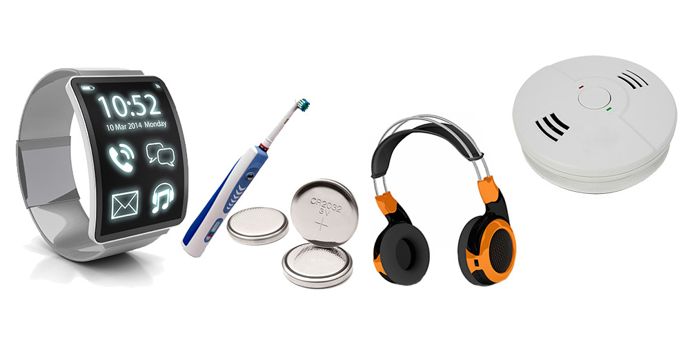
A: Over the past decade, we have observed growing pressure to control the rising cost of healthcare. Opportunities brought about by this pressure include a trend toward evidence-based medicine. This trend necessitates new medical devices that can sense, analyze, communicate, and store personalized health indicators. These new devices promise to eliminate subjectivity and human error, resulting in more accurate, effective, and economical treatments. The evidence-based medicine trend coincides with a trend toward more real-time and continuous diagnostics. These goals can typically only be met with wearable or implantable devices, which frequently require the types of custom IC products that Cactus Semiconductor provides.
Another significant opportunity is the trend toward implantable device miniaturization. Through device miniaturization, we enable minimally invasive implant surgeries that are performed in outpatient clinics instead of hospitals, reduce the risks of complications and infections, and expedite healing. Overall, device miniaturization can lead to significantly more cost-effective solutions.
 Recommended: Digital Harbor: Incubating The Future With Conversational Applications
Q: What are your plans for the future?
A: Our plans for the future include continued growth of our ASIC business, to establish ourselves as the premier provider of medical device ASICs worldwide. Other plans include an expansion of our capabilities into tangential markets that fit well with our current experience and expertise. For example, some recent projects include Wireless Communication and Energy Harvesting ASICs. These types of products are also critical parts of the booming Internet of Things (IoT) market. Most of these IoT applications present challenges similar to those faced by our medical device ASICs. Specifically, they require complex power management and aggressive miniaturization. Cactus believes that we are well-positioned to participate in those end markets, and plan to continue our growth in those areas.
Activate Social Media: